MARION SYSTEMS CORP,
Santa Monica, CA 90401
MS68K
SINGLE BOARD
COMPUTER
User's Manual
Table of Contents
GENERAL DESCRIPTION
MS68K SPECIFICATIONS
PARTS LAYOUT
SYSTEM INTEGRATION
Introduction
Power
Terminal
Modem
Floppy
SCSI
Parallel Printer
Expansion Bus
Jumpers
TECHNICAL DESCRIPTION
Introduction
68000 Microprocessor and Memory Map
Clock and Reset
Memory and Peripheral Device Decoding
ROM Memory
RAM Memory
Interrupts
DTACK and Bus Error
Addressing of Eight Bit Peripherals
DUART and Serial Channels
Floppy
Printer
SCSI
Expansion Bus
ROM MONITOR
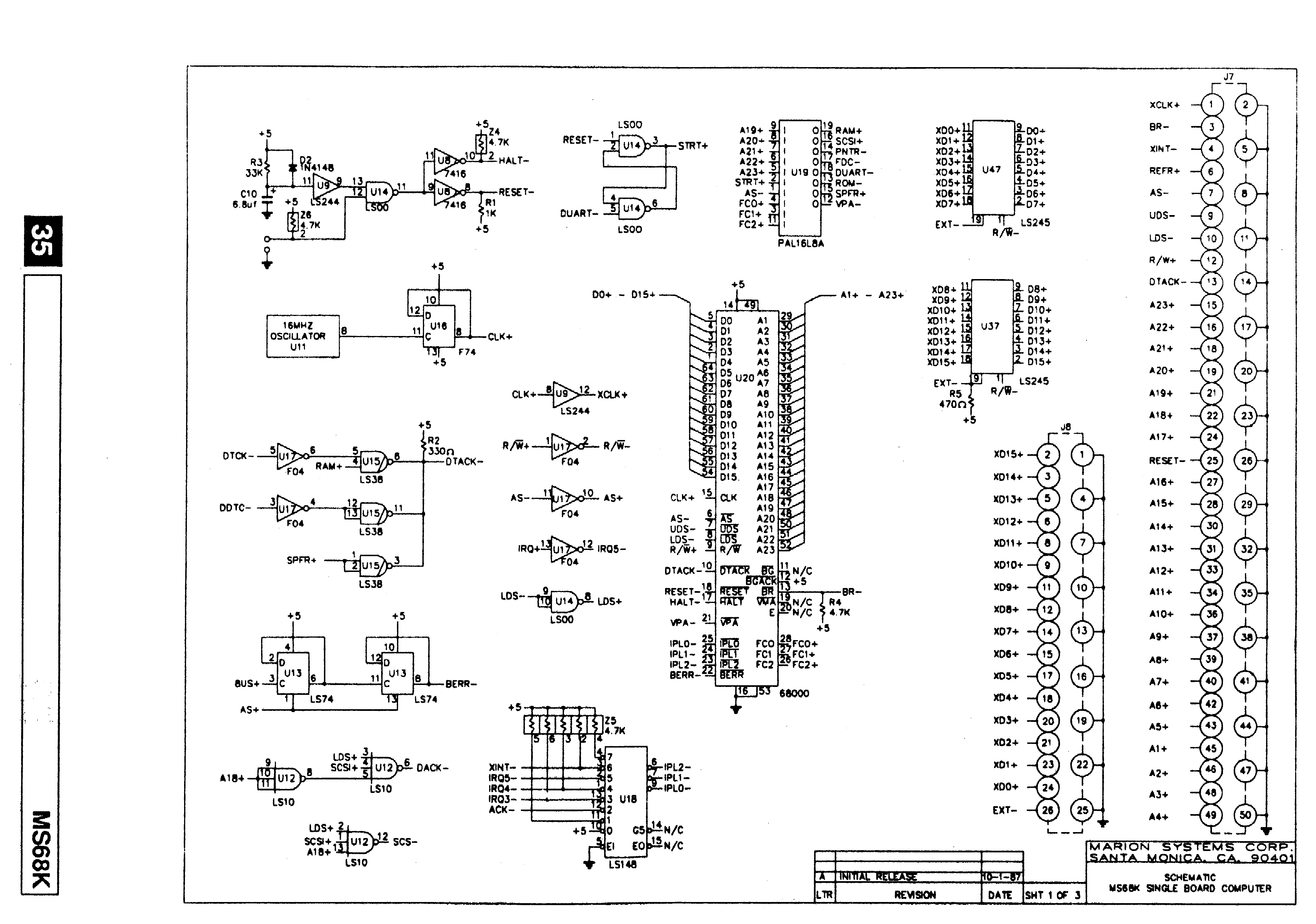
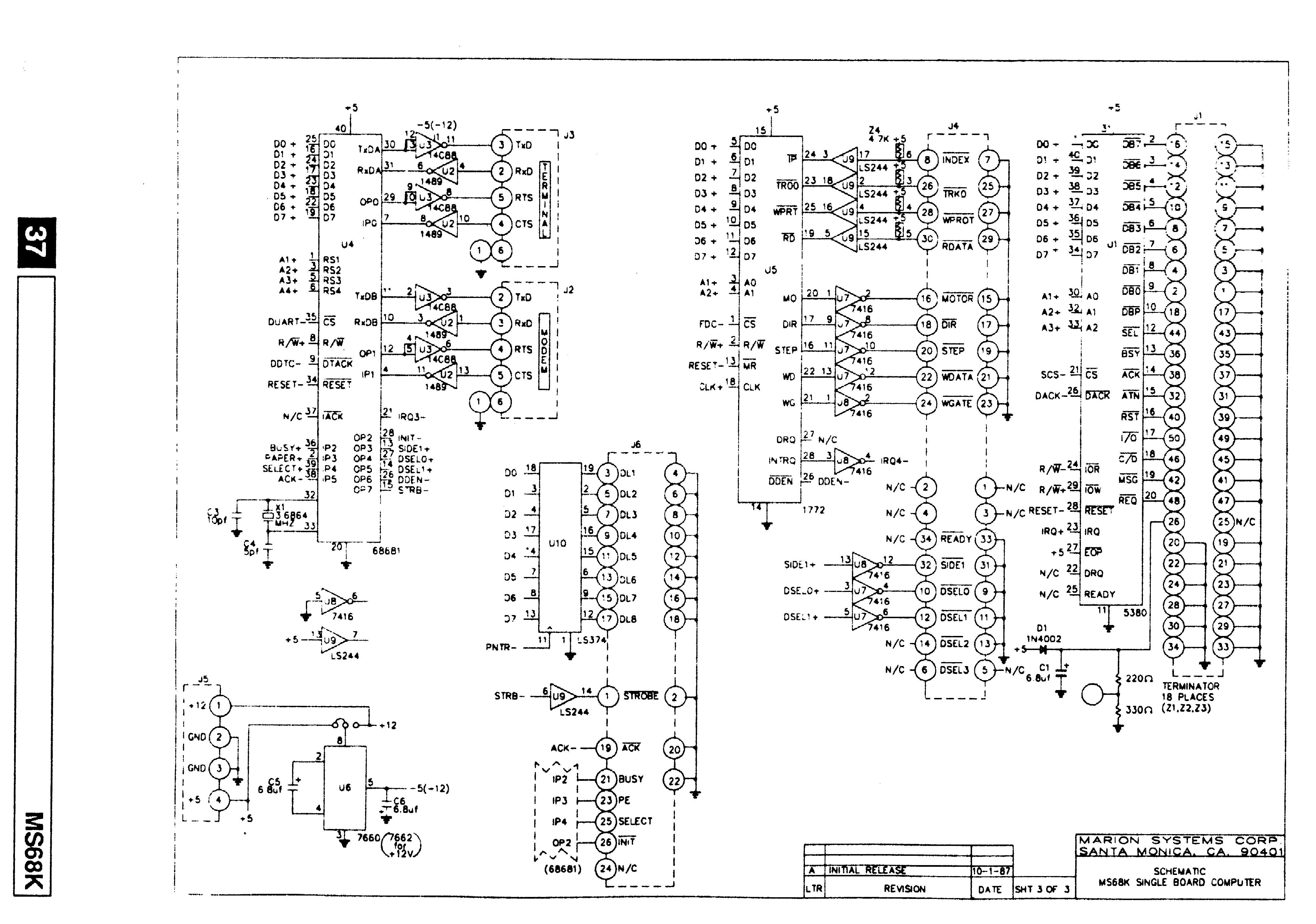
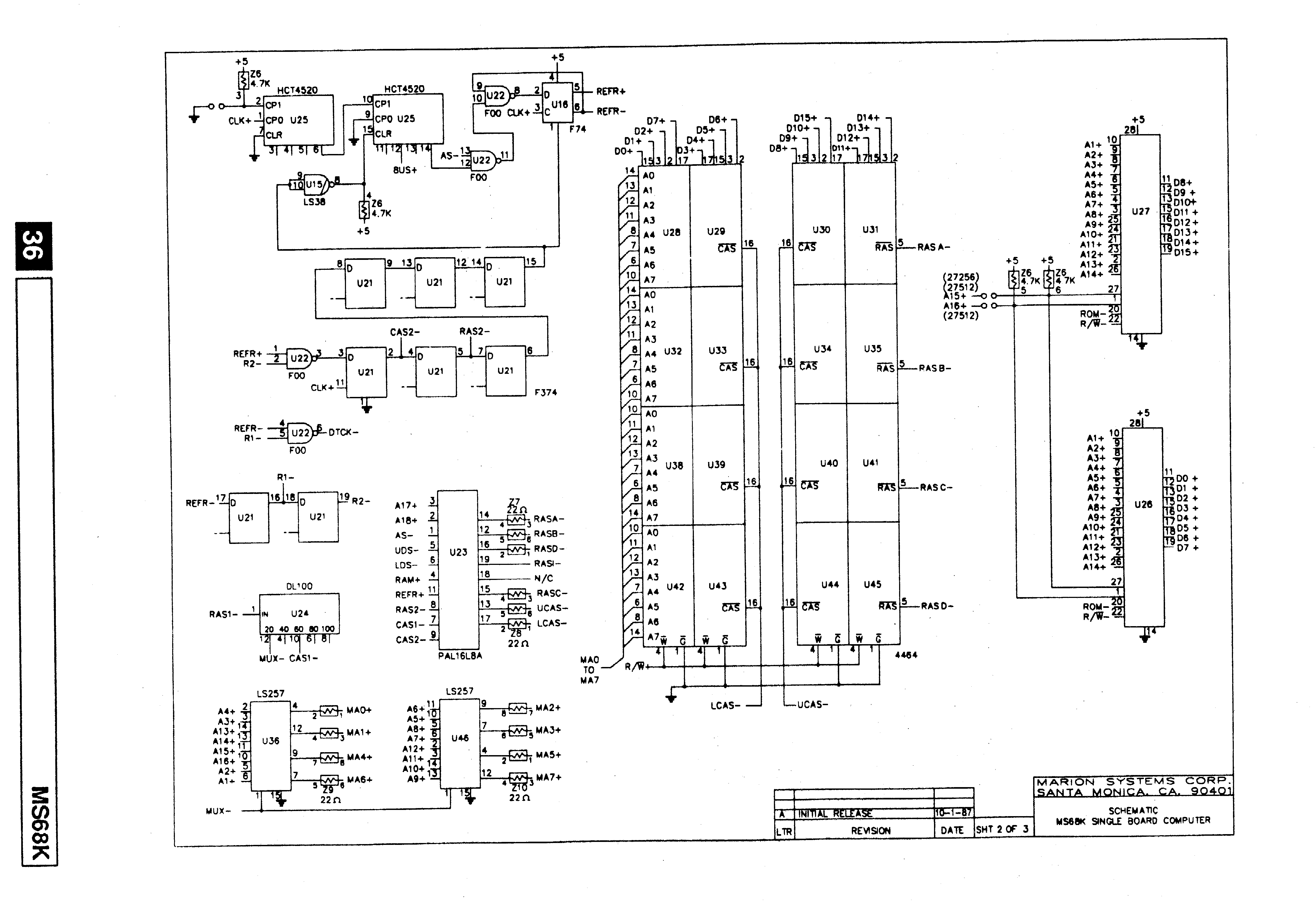
SCHEMATICS
General Description
The Marion Systems MS68K Single Board Computer is a complete
68000 microprocessor-based computer system on a compact 5- 3/4"
by 8" printed circuit board. In addition to the 68000 microprocessor
running at 8 MHz, the MS68K also has on board support for up to
512K bytes of DRAM, up to 128K bytes of EPROM, controllers for
floppy and hard disks, two serial ports, a parallel port and a com
plete expansion bus. It requires only +5 volts DC power to operate.
All of the basic elements of a complete microprocessor based system
arc included on the MS68K board. The 68000 microprocessor is the
same powerful CPU which is used in numerous popular computers
and engineering workstations. The MS68K can contain up to 512K
bytes of no wait state dynamic RAM, which is adequate for a great
many applications. For systems requiring more memory, Memory
Expansion Boards are available which allow the user to configure
systems with up to 12.5 megabytes of memory.
The MS68K contains sockets which accept up to 128K bytes of
EPROM storage. EPROM types 2764 thru 27512 can be accommo
dated.
Included with each MS68K is a very complete ROM monitor
contained on two 27128 EPROMs. In addition to the standard
debugging features backtracking, tracing execution, and chang
ing, listing, moving and searching memory. The ROM monitor also
contains a line assembler and line disassembler.
For serial port communication, the MS68K utilizes the popular
68681 interface circuit, which provides one serial port for a CRT
terminal, plus a second serial port for a modem or serial printer.
The 68681 also provides a 16-bit counter-timer.
For controlling mass storage, the MS68K has the capability of inter
facing to both floppy disks and hard disks. Unique to boards of its
type, the MS68K contains a socket for a 5380-type SCSI protocol
controller, which can control hard disks of various sizes, as well as
providing general-purpose, bidirectional input-output. In addition,
the MS68K includes a 1772- type floppy controller for interfacing up
to two 3 1/2" or 5 1/4" floppy drives.
Completing the extensive I/O capabilities of the MS68K is a standard
parallel printer port and a complete expansion bus. The expansion
bus is designed for additional boards to be interfaced to the MS68K,
allowing complex systems to be formulated. Marion Systems
provides Memory Expansion Boards which interface to the MS68K
thru the expansion bus and provide up to 12 megabytes of additional
RAM memory
MS68K Specifications
Processor
CPU:6800016/32 Bit microprocessor
Clock:8 MHz
Memory
DRAM
256K bytes dynamic RAM
0 wait state
Expandable to 512K bytes on board
EPROM
Up lo 128K bytes of EPROM
Accommodates 2764 thru 27512 type EPROM
ROM Monitor
Two 27128 EPROMs
Extensive debug facilities including line
assembler and disassembler, trace; set/clear
breakpoints, change, list, move, search memory
download programs, etc.
Expansion
Up to total system RAM of 12.5 megabytes
Disk Control
SCSI
5380-type SCSI protocol controller
Interfaces various sizes of hard disks
Floppy
1772-type floppy controller
Interfaces two 3 1/2" or 5 1/4" floppy disks
Input/Output
Serial:
Two serial ports using 68681 controller
Programmable baud rates to 38.4 kilobaud
Programmable handshake
Parallel
Industry standard printer interface
Expansion Bus
76 pin high speed expansion bus
Includes all data and address line,
all strobes, system clock, interrupt
line, memory refresh control, etc.
Power DC Power +5 volts @ IS amp
Dimensions
5 3/4" X 8
Mounts on 5 1/4" disk drive

System Integration
Introduction
The MS68K can be the heart of a very powerful and capable
system, however in its most basic form a simple system consists
-MS68K Single Board Computer with ROM Monitor
-ASCII Terminal
-Power Supply
To this basic system other components can be added - such as
floppy disks, SCSI hard disks, modems, printers, expansion
cards - to build your desired configuration. The following
sections describe how to integrate these various components
into your system. Refer to Figure 1 for the locations of the
various connectors.
Power
The MS68K requires only +5 volts DC at 1.5 amps to operate. It
uses a connector which is identical to those used on most 5 1\4"
floppy and hard disks.
CAUTION
BE VERY CAREFUL BEFORE APPLYING POWER
TO THE MS68K. MAKE SURE THAT YOUR
POWER CABLE IS WIRED CORRECTLY |
.
Table l. Power Connector (J5)
| PIN | NAME | Description |
| 1 | +12 | +12 Volts DC (Optional) |
| 2 | Ground | +12 Volt Return |
| 3 | Ground | +5 Volt Return |
| 4 | +5 | +5 volts DC |
Mating Connector:AMP 1-480424-0
Mating Pins:AMP 60617-1
(Supplied in MS68K Accessory Kit)
Terminal
A console terminal is required for basic operation of the MS68K.
The terminal communicates with the MS68K by means of an RS-232
serial interface thru Port A. the Terminal Port A 68681 DUART
(Dual Universal Asynchronous Receiver Transmitter) performs the
functions of serial/parallel conversion and other tasks required
for RS-232 communication. When power is applied or a system reset
is forced, the ROM Monitor initializes Port A of the DUART as
follows:
-9600 Baud
-1 Stop Bit
-8 Bits per Character
-No Parity
TABLE 2 Terminal Connector (J3)
| Pin | Name | Description | In/Out |
| 1 | Ground | Ground | -- |
| 2 | RxD | Received Data | In |
| 3 | TxD | Transmitted Data | Out |
| 4 | CTS | Clear To Send | In |
| 5 | RTS | Request To Send | Out |
| 6 | Ground | Ground | -- |
Mating Connector: MOLEX 22-01-2061
Mating Pins: MOLEX 08-50-0114
(Supplied in MS68K Accessory Kit)
Figure 2 - TYPICAL TERMINAL CABLE
CABLE
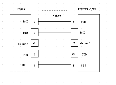
(wires within dotted lines nay be required for > 9600 baud)
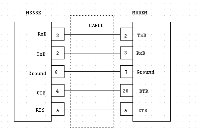
Modem
The DUART on the MS68K furnishes a second serial port in
addition to the port used for the terminal, and this port can be
used to interface a modem, serial printer, or other RS-232 serial
device. When power is applied or a system reset is forced, the
ROM Monitor initializes Port B of the DUART as follows:
-1200 Baud
- 1 Stop Bit
- 8 Bits per Character
- No Parity
The ROM Monitor can be used to change the baud rate of Port B
table 3. Modem Connector (J2)
| PIN | NAME | DESCRIPTION | In/Out |
| 1 | Ground | Ground | -- |
| 2 | TxD | Transmitted Data | Out |
| 3 | RxD | Received Data | In |
| 4 | RTS | Reqeust To Send | Out |
| 5 | CTS | Clear To Send | In |
| Ground | Ground | -- |
Mating Connector: MOLEX 22-01-2061
Mating Pins: MOLEX 08-50-0114
(Supplied in MS68K Accessory Kit)
Figure 3 - typical modem cable
Floppy
The MS68K utilizes a 1772-typc (floppy controller to interface up
to two 5 1\4" or 3 1\2" floppy drives. Basically any type of
floppy drive which is soft-sectored, single or double density,
40 or 80 track will work with the MS68K. The floppy drives
interface to the system by means of a power cable and a signal
cable. Most 5 1\4" floppy drives require a power cable with
connections similar to those shown in Table 1. However,
3 1\2" floppy drives generally require a different power
connector than those for 5 P4N drives. Consult your particular
drive specification for details.
The signal cable required for your particular system will depend
upon the type of floppy drives you have chosen. The signal
connector on most 5 1VT floppy drives is a printed circuit edge
connector and requires a mating connector such as:
MOLEX 15-29-0341
3M 3463-0001
The signal connector of most 3 1\2" floppy drives is a ribbon
cable type. Typical mating connectors are:
AMP 499496-9
MOLEX 15-29-8342
Note:
On
certain 3-1/2" drives, the mechanical keying on the drive itself is such
that the "V- mark" which normally designates Pin 1 willinstead be designating Pin 34.
|
If you are connecting only one floppy drive to your system make
sure that it has only the "Drive Select 0" jumper installed, and
has the terminating resistors installed. If you are interfacing
two drives, one drive should only have its "Drive Select 0'jumper
installed and the second drive should only have its "Drive
Select 1" jumper installed. In addition, make sure that only
the drive at the end of the signal cable, farthest from the MS68K,
has its terminating resistors installed.
Floppy
Table 4 Floppy Connector (J4)
| Pin | Name | Description | In/Out |
| 2 | --- | (NOT USED) | --- |
| 4 | --- | (NOT USED) | --- |
| 6 | --- | (NOT USED) | --- |
| 8 | INDEX- | INDEX PULSE | IN |
| 10 | DSEL0 | DRIVE SELECT 0 | OUT |
| 12 | DSEL1 | DRIVE SELECT 1 | OUT |
| 14 | --- | (NOT USED) | --- |
| 16 | MOTOR- | MOTOR ON | OUT |
| 18 | DIR- | STEP DIRECTION SELECT | OUT |
| 20 | STEP- | STEP | OUT |
| 22 | WDATA- | WRITE DATA | OUT |
| 24 | WGATE- | WRITE GATE | OUT |
| 26 | TRK0- | TRACK 0 STATUS | IN |
| 28 | WPROT- | WRITE PROTECT STATUS | IN |
| 30 | RDATA- | READ DATA | IN |
| 32 | SIDE1- | SIDE ONE SELECT | OUT |
| 34 | --- | (NOT USED) | --- |
| 7-33 (odd pins) | GND | SIGNAL GROUND | --- |
Mating Connector: amp 499496-9
SCSI Interface
The SCSI interface allows the MS68K to communicate with a variety
of SCSI-compatible devices, such as hard disks, tape drives,
printers, other computer systems, etc. In addition, the SCSI
interface can be used as a general purpose, 8-bit input-output
The SCSI interface consists of 18 signals on a 50-pin connector.
All signals are bidirectional, active low, can drive/must be
driven by open-collector drivers with 48 mA. sink capability.
All 18 signals are terminated on the MS68K by a 220 ohm resistor
to 5 and a 330 ohm resistor to ground.
TABLE 5 scsi Connector (J1)
| PIN | NAME | DESCRIPTION | IN/OUT |
| 2 | DB0- | Data Bit 0 (LSB) | In/Out |
| 4 | DB1- | Data Bit 1 | In/Out |
| 6 | DB2- | Data Bit 2 | In/Out |
| 8 | DB3- | Data Bit 3 | In/Out |
| 10 | DB4- | Data Bit 4 | In/Out |
| 12 | DB5- | Data Bit 5 | In/Out |
| 14 | DB6- | Data Bit 6 | In/Out |
| 16 | DB7- | Data Bit 7 (MSB) | In/Out |
| 18 | DBP- | Data Parity Bit | In/Out |
| 20 | GND | ground | --- |
| 22 | GND | ground | --- |
| 24 | GND | ground | --- |
| 26 | TERMPWR | Terminator Power | --- |
| 28 | GND | ground | --- |
| 30 | GND | ground | --- |
| 32 | ATN- | Attention | In/Out |
| 34 | GND | ground | --- |
| 36 | BSY- | Busy | In/Out |
| 38 | ACK- | Acknowledge | In/Out |
| 40 | RST- | SCSI Bus reset | In/Out |
| 42 | MSG- | Message | In/Out |
| 44 | SEL- | Select | In/Out |
| 46 | C/D- | Control/Data | In/Out |
| 48 | REQ- | Request | In/Out |
| 50 | I/O- | Input/Output | In/Out |
| 1-23 | GND | ground | --- |
| 25 | --- | (Not Used) | --- |
| 27-49 | GND | ground | --- |
Mating Connector
AMP 1-499496-2
MOLEX 15-29-8502
Parallel Printer
The parallel printer port allows a printer with a Centronics-type
interface to be driven by the MS68K. The interface on the MS68K
is a 26-pin connector that is configured for popular printer ribbon
cables, such as the Radio Shack # 26-1409. Since the connector
that is used for connecting to printers has a different pin
numbering scheme, the pin numbers on the MS68K connector (J6)
do not match the pin numbers on the printer. This is shown in the
following table.
table 6. Parallel Print (J6)
Cent
Pin | J6 Pin | Name | Description | In/Out |
| 1 | 1 | STROBE - | DATA STROBE | OUT |
| 2 | 3 | DL1 | DATA LINE 1 (LSB) | OUT |
| 3 | 5 | DL2 | DATA LINE 2 | OUT |
| 4 | 7 | DL3 | DATA LINE 3 | OUT |
| 5 | 9 | DL4 | DATAA LINE 4 | OUT |
| 6 | 11 | DL5 | DATA LINE 5 | OUT |
| 7 | 13 | DL6 | DATA LINE 6 | OUT |
| 8 | 15 | DL7 | DATA LINE 7 | OUT |
| 9 | 17 | DL8 | DATA LINE 8 | OUT |
| 10 | 19 | ACK- | ACKNOWLEDGE | IN |
| 11 | 21 | BUSY | PRINTER BUSY | IN |
| 12 | 23 | PE | PAPER END | IN |
| 13 | 25 | SELECT | SELECT | IN |
| 31 | 26 | INIT- | INITIALIZE PRINTER | OUT |
| 30 | 24 | --- |
| --- |
19-29
(odd) | 2-22
(even) | GND | Ground | --- |
MS68K Mating Connector : MOLEX 15-29-8262
AMP 499495-7
Printer Mating Connector : Amphenol 57-30360
Expansion Bus
The MS68K expansion bus allow the integration of a wide variety
of external devices to the MS68K. This bus is basically an
interface to and from the 68000 microprocessor, with the
addition of certain signals to make the bus more general
purpose.
TABLE 7. Expansion Bus (J8)
| Pin | Name | Description | In/Out |
| 1 | GND | Ground | --- |
| 2 | XD15+ | Ext Data Bit 15 | In/Out |
| 3 | XD14+ | Ext Data Bit 14 | In/Out |
| 4 | GND | Ground | --- |
| 5 | XD13+ | Ext Data Bit 13 | In/Out |
| 6 | XD12+ | Ext Data bit 12 | In/Out |
| 7 | GND | Ground | --- |
| 8 | XD11+ | Ext Data Bit 11 | In/Out |
| 9 | XD10+ | Ext Data Bit 10 | In/Out |
| 10 | GND | Ground | --- |
| 11 | XD9+ | Ext Data Bit 9 | In/Out |
| 12 | XD8+ | Ext Data Bit 8 | In/Out |
| 13 | GND | Ground | --- |
| 14 | XD7+ | Ext Data Bit 7 | In/Out |
| 15 | XD6+ | Ext Data Bit 6 | In/Out |
| 16 | GND | Ground | --- |
| 17 | XD5+ | Ext Data Bit 5 | In/Out |
| 18 | XD4+ | Ext Data Bit 4 | In/Out |
| 19 | GND | Ground | --- |
| 20 | XD3+ | Ext Data Bit 3 | In/Out |
| 21 | XD2+ | Ext Data Bit 2 | In/Out |
| 22 | GND | Ground | --- |
| 23 | XD1+ | Ext Data Bit 1 | In/Out |
| 24 | XD0+ | Ext Data Bit 0 | In/Out |
| 25 | GND | Ground | --- |
| 26 | EXT- | External Select | In |
J8 Mating Connector: AMP 1-499496-2
(50 pin) MOLEX 15-29-8502
J7 Mating Connector: AMP 499495-7
(26 pin) MOLEX 15-29-8262
TABLE 8 Expansion Bus (J7)
| Pin | Name | Description | In/Out |
| 1 | XCLK+ | 8 MHz Buffered Cpu Clock | Out |
| 2 | GND | Ground | --- |
| 3 | BR- | Bus Request | In |
| 4 | XINT- | External Interrupt | In |
| 5 | GND | Ground | --- |
| 6 | REFR+ | Refresh | Out |
| 7 | AS- | Address Strobe | Out |
| 8 | GND | Ground | --- |
| 9 | UDS- | Upper Data Strobe | Out |
| 10 | LDS- | Lower Data Strobe | Out |
| 11 | GND | Ground | --- |
| 12 | R/W+ | Read / Not Write | Out |
| 13 | DTACK- | Data Transfer Acknowledge | Out |
| 14 | GND | Ground | --- |
| 15 | A23+ | Address Bus Bit 23 | Out |
| 16 | A22+ | Address Bus Bit 22 | Out |
| 17 | GND | Ground | --- |
| 18 | A21+ | Address Bus Bit 21 | Out |
| 19 | A20+ | Address Bus Bit 20 | Out |
| 20 | GND | Ground | --- |
| 21 | A19+ | Address Bus Bit 19 | Out |
| 22 | A18+ | Address Bus Bit 18 | Out |
| 23 | GND | Ground | --- |
| 24 | A17+ | Address Bus Bit 17 | Out |
| 25 | RESET- | Master Reset | Out |
| 26 | GND | Ground | --- |
| 27 | A16+ | Address Bus Bit 16 | Out |
| 28 | A15+ | Address Bus Bit 15 | Out |
| 29 | GND | Ground | --- |
| 30 | A14+ | Address Bus Bit 14 | Out |
| 31 | A13+ | Address Bus Bit 13 | Out |
| 32 | GND | Ground | --- |
| 33 | A12+ | Address Bus Bit 12 | Out |
| 34 | A11+ | Address Bus Bit 11 | Out |
| 35 | GND | Ground | --- |
| 36 | A10+ | Address Bus Bit 10 | Out |
| 37 | A9+ | Address Bus Bit 9 | Out |
| 38 | GND | Ground | --- |
| 39 | A8+ | Address Bus Bit 8 | Out |
| 40 | A7+ | Address Bus Bit 7 | Out |
| 41 | GND | Ground | --- |
| 42 | A6+ | Address Bus Bit 6 | Out |
| 43 | A5+ | Address Bus Bit 5 | Out |
| 44 | GND | Ground | --- |
| 45 | A1+ | Address Bus Bit 1 | Out |
| 46 | A2+ | Address Bus Bit 2 | Out |
| 47 | GND | Ground | --- |
| 48 | A3+ | Address Bus Bit 3 | Out |
| 49 | A4+ | Address Bus Bit 4 | Out |
| 50 | GND | Ground | --- |
Clock and Reset
The master timing for the MS68K is an 8 MHz clock. This signal
is derived from a 16 MHz oscillator which is divided by two.
The resulting 8 MHz signal drives both the 68000 microprocessor
and the 1772 floppy disk controller. t.
The MS68K system is reset whenever power is applied, and this
causes the appropriate circuitry to be initialized, the ROM
memory to be mapped to the start of memory, and RAM memory to
be disabled. This is done so that the 68000 microprocessor can
initially load its stack pointer and program counter with
starting values. In this case, the program counter is loaded -
with the starting address of the ROM Monitor. When the reset :
function has terminated, the 68000 microprocessor starts
executing instructions in the ROM Monitor. One of the first
instructions that is executed is an instruction which accesses
the DUART. This action automatically remaps the ROM to upper
memory and enables RAM addressing.
Memory and Peripheral Device Decoding
All memory and peripheral devices exist in the memory space of
the 68000 microprocessor since it does not have separate
input/output instructions. These addresses are decoded by a PAL
programmed logic device. The decoded addresses are as follows:
| Styart Address | End Address | Device |
| $000000 | $07FFFF | Ram Memory (first 512K bytes) |
| $D00000 | $D7FFFF | SCSI Controller |
| $D80000 | $DFFFFF | Parrallel Printer Controller |
| $E00000 | $E7FFFF | Floppy Disk Controller |
| $E80000 | $EFFFFF | DUART Serial Controller |
| $F00000 | $F7FFFF | Rom Monitor |
In addition, the PAL generates the signal VPA- which is used as
part of the interrupt acknowledge process by instructing the
68000 microprocessor to use autovcctored interrupts.
The logic equations for the memory decode PAL are given below
RAM = A23- * A22- * A21- * A20- * A19- * STRT-
SCSI = A23+ * A22+ * A21- * A20+ * A19-
PNTR = A23+ * A22+ * A21- * A20+ * A19+ * AS+
FDC = a23+ * A22+ * A21+ * A20- * A19- * AS+
DUART = A23+ * A22+ * a21+ * a20- * a19+ * AS+
ROM = A23+ * A22+ * A21+ * A20+ * A19- | STRT+
SPFR = SCSI+ | PNTR+ | FDC+ | ROM+
VPA = FC0+ * FC1+ * FC2+ * AS+
Where * = Logical AND
+ = Active High
- = Act6ive Low
| = Logical OR
ROM Memory
The MS68K can accommodate ROM (EPROM) memory as described
below:
| Eprom Type | Size (2 Eproms) | Jumper |
| 2764 | 16K Bytes | --- |
| 27128 | 32 K Bytes | --- |
| 27256 | 64 K Bytes | 1 |
| 27512 | 128 K Bytes | 2 |
The EPROM access time must be 250 nanoseconds or better.
RAM Memory
The basic MS68K system comes with 256K bytes of dynamic RAM which
can be expanded on board to 512K bytes. Memory expansion can be
accomplished by the user by installing appropriate memory chips
on the MS68K board. The DRAM chips used in the MS68K arc 64K by
4 types with an access time of 150 nanoseconds. Some acceptable
DRAMs are:
| DRAM Type | Manufacturer |
| HM50464p-15 | Hitatchi |
| NEC D41464C-15 | NEC |
| TMS4464-15NL | Texas Instruments |
| TMM 41464P-15 | Toshiba |
Dynamic memory chips require periodic refresh for data retention
This refresh operation is performed on the MS68K by circuitry
which operates independently of the 68000 microprocessor. The
memory chips are refreshed using the "CAS before RAS" refresh
method. The 8 MHz system clock is counted down by a refresh
counter. When this counter indicates that 16 microseconds has
elasped since the last refresh cycle, the refresh circuitry is
armed and waits until the present memory cycle has terminated.
When this occurs, a refresh command flip-flop is set, indicating
a refresh cycle is to take place. While this is occurring, the
microprocessor DTACK- signal is negated, which causes the next
memory cycle to be delayed until the refresh cycle is completed.
In order to simplify the implementation of expansion memory
external to the MS68K board, this refresh command flip-flop
signal is provided on the expansion bus.
Interrupts
There are five sources of interrupts to the 68000 microprocessor
These interrupts are, in order of highest priority to lowest
priority:
| Interrupt Source | 68000 Priority Level |
| External Interrupt (expansion bus) | 6 |
| SCSI Interrupt | 5 |
| Floppy Interrupt | 4 |
| DUART Interrupt | 3 |
| Printer Interrupt | 2 |
These signals are prioritized and encoded into the three signals,
IPLO-2 (which are required by the microprocessor), by a 74LS148
priority encoder circuit If a device is requesting an interrupt
at a priority level higher than the interrupt mask contained in
the microprocessor's status register, it will be serviced when the
microprocessor completes the present instruction. The micro-
processor responds by jumping to the address contained in the
exception vector table "autovector" location associated with the
interrupting device's priority level This is a consequence of
the PAL device responding to the microprocessor's interrupt
acknowledge by asserting the VPA signal.
DTACK and Bus Error
Built into the 68000 microprocessor is a mechanism which allows
it to work with memories and peripherals of various speeds. The
DTACK- input to the microprocessor can be used to effectively
"stall** the microprocessor when an addressed device cannot
respond in the minimum time allowed during instruction
execution. Each addressed device must generate the DTACK- signal
when it either has data ready for the 68000 or is ready to
receive data from it.
If the microprocessor attempts to access a non-existent device,
no DTACK- will be returned and the system could hang. To prevent
this situation, the microprocessor has an input, BERR- (bus
error), which when asserted causes an interrupt This signal is
driven by a timer which is allowed to count when the microprocessor
is attempting to access a device. If no device responds after a
certain time, the Bus Error signal is asserted. From the time a
microprocessor bus cycle begins until Bus Error is asserted is
a minimum 8 microseconds.
Addressing of Eight Bit Peripherals
The input/output peripherals on the MS68K are eight bit
peripherals existing in a 16-bit environment Therefore, it is
necessary to decide whether their data buses are connected to
the upper or lower eight bits of the 68000 microprocessor.
By convention, eight bits peripherals are usually connected
to the lower eight bits (DO thru D7, and consequently their
memory addresses appear as odd addresses. For instance, as the
memory map shows, the block of memory assigned to the parallel
printer port is SD80000. However, when actually addressing
the printer byte buffer in a program, one would use SD80001
as it s access address.
DUARTand Serial Channels
The MS68K utilizes a 68681 DUART chip for serial communication
with the system terminal and an optional modem or serial
printer. TTiis DUART chip also provided six parallel input
and eight parallel output lines. Some of the features of this
device are:
- Two independent full-duplex serial channels
- Internal programmable baud rate generators for each
channel with baud rates up to 38.4 Kbaud
-Buffered input/output
- Programmable serial transmission formats
- Six bit parallel input port
- Eight bit parallel output port
- Interrupt logic compatible with 68000 interrupts
- 16-bit programmable counter/timer
The input/output capabilities of the 68681DUART consist of both
serial and parallel interfaces. The serial channels are used,
as mentioned above, for terminal and modem interfacing. The
uses of the parallel input and output ports are summarized in the
tables on the following page.
Uses of the Parallel Input and Output Ports
Input
Bit
|
Device
|
Function
|
IP0
|
Terminal
|
Clear To Send
|
IP1
|
Modem
|
Clear To Send
|
IP2
|
Printer
|
Busy
|
IP3
|
Printer
|
Paper Out
|
IP4
|
Printer
|
Device Selected
|
IP5
|
Printer
|
Acknowledge
|
Output
Bit
|
Device
|
Function
|
OP0
|
Terminal
|
Requesest To Send
|
OP1
|
Modem
|
Request To Send
|
OP2
|
Printer
|
Initialize
|
OP3
|
Floppy
|
Side One Select
|
OP4
|
Floppy
|
Drive Select 0
|
OP5
|
Floppy
|
Drive Select 1
|
OP6
|
Floppy
|
Double Density
|
OP7
|
Printer
|
Data Strobe
|
Programming of the DUART and data communication between it
and the microprocessor is accomplished by the microprocessor
reading and writing registers within the DUART. The names of
these registers and addresses are listed in tables 9 and 10.
For further information regarding the use and programming of the
68681 DUART, refer to either of the following documents:
MC68681 Dual Asynchronous ReceiverlTransmitter
Data Book ADI988R1
Motorola Semiconductor, Austin, TX
SCN68681 Dual Asynchronous Receiver/Transmitter
Microprocessor Data Manual
Signetics Corporation, Sunnyvale, CA
Table 9. 68681 duart Read-only Registers
Address
|
Function
|
Name
|
$E80001
|
Mode Register A
|
MR1A
MR2A
|
$E80003
|
Status Register A
|
SRA
|
$E80005
|
(do NOT use)
|
|
$E80007
|
Reciever Buffer A
|
RBA
|
$E80009
|
Input Port Change Register
|
IPCR
|
$E8000B
|
Interrupt Status Register
|
ISR
|
$E8000D
|
Counter Mode:Current MSB of Counter
|
CUR
|
$E8000F
|
Counter Mode:Current LSB of Counter
|
CLR
|
$E80011
|
Mode Register B
|
MR1B
MR2B
|
$E80013
|
Status Register B
|
SRB
|
$E80015
|
Do Not Use
|
|
$E80017
|
Reciever Buffer B
|
RBB
|
$E80019
|
Interrupt Vector Register
|
IVR
|
$E8001B
|
Input Port (unlatched)
|
|
$E8001D
|
Start Counter Command (address triggered)
|
|
$E8001F
|
Stop Counter Command (address triggered)
|
|
Table 10. 68681 doart write-only Registers
Address
|
Function
|
Name
|
$E80001
|
Mode Register A
|
MR1A,MR1B
|
$E80003
|
Clock Select Register
|
CSRA
|
$E80005
|
Command Register A
|
CRA
|
$E80007
|
Transmit Buffer A
|
TBA
|
$E80009
|
Auxiliary Control Register
|
ACR
|
$E8000B
|
Interrupt Mask Register
|
IMR
|
$E8000D
|
Counter Timer Upper Register
|
CTIUR
|
$E8000F
|
Counter Timer Lower Register
|
CTLR
|
$E80011
|
Mode Register B
|
MR1B,MR2B
|
| $E80013 |
Clock Select Register B
|
CSRB
|
| $E80015 |
Command Register B
|
CRB
|
| $E80017 |
Transmit Buffer B
|
TBB
|
| $E80019 |
Interrupt Vector Register
|
IVR
|
| $E8001B |
Output Port Configuration Register
|
OPCR
|
| $E8001D |
Output Port Bit Set Command
|
|
| $E8001F |
Output Port Bit Reset Command
|
|
Floppy
The MS68K utilizes the Western Digital 1772 floppy controller to
interface either one or two floppy drives to the 68000 micro-
processor. This chip includes all the circuitry necessary to
interface the drives except for bus drivers and receivers, and
the density, side and drive select signals. All of the functions
involving floppy disk operation are controlled by the proper
programming of the 1772. This is accomplished by reading and
writing registers within the 1772 that are addressable by the
68000 microprocessor. The 1772 registers and their addresses
are listed below:
Register
|
Address
|
Status Register
|
$E00001 (read only)
|
Command Register
|
$E00001 (write only)
|
Track Register
|
$E00003
|
Sector Register
|
$E00005
|
Data Register
|
$E00007
|
Notice that the status register is read-only and the command
register is write-only, and therefore they share the same address.
The signals which control density, side select and drive select
originate from the 68681 DUART output port .The output port bits
in the DUART require separate commands for setting and resetting.
This fact, combined with logical inversion within the DUART of the
output bits and inverters on the side and drive select lines, can
cause confusion as to how these functions are selected. This
is accomplished as summarized below:
Output
Bit
|
Function
|
68000 Instruction
|
OP3
|
Select Side 0
Select Side 1
|
move.b #$08,$E8001D
move.b #$08,$E8001F
|
OP4
|
Select Drive 0
DeSelect Drive 0
|
move.b #$10,$E8001F
move.b #$10,$E8001D
|
OP5
|
Select Drive 1
DeSelect Drive 1
|
move.b #$20,$E8001F
move.b #$20,$E8001D
|
OP6
|
Select Single Density
Select Double Density
|
move.b #$40,$E8001F
move.b #$40,$E8001D |
Prior to performing the above set and reset commands, the
output port configuration register must be cleared to all
zeroes with the following instruction:
move.b #$00,$E8001B
Since there is a bit assigned separately to each function, it is
possible to use a combination which sets the appropriate bits,
and a combination which resets the appropriate bits, as in the
following example:
Example: Configure the 1772 for Side 0,
Drive 0 and Double Density
move.b #$68,$E8001D Set bits 0P3, 0P5 and 0P6
move.b #$10,$E8001F Reset bit 0P4
For further information regarding the use and programming of the
1772 floppy controller, refer to the following document:
WD177X-00 Floppy Disk Formatter/Controller
Storage Management Products Handbook
Western Digital Corporation, Irvine, CA
Printer
The MS68K parallel printer interface is compatible with the
industry standard Centronics interface, and includes eight data
lines with a strobe and an initialize signal which drive the
printer, and four status lines from the printer. A summary of
the signals and their sources is given below:
Signal
|
Description
|
Source
|
STROBE-
|
DATA STROBE
|
74LS244/MC68681
|
DL1-> DL8
|
DATA LINES
|
74LS374
|
INIT-
|
INITIALIZE
|
MC68681
|
ACK-
|
ACKNOWLEDGE
|
PRINTER
|
BUSY
|
PRINTER BUSY
|
PRINTER
|
PE
|
PAPER END
|
PRINTER
|
SELECT
|
SELECT
|
PRINTER
|
The STROBE- and INIT- signals originate from the 68681 DUART
output port The output port bits in the DUART require separate
commands for setting and resetting. This fact, combined with
logical inversion within the DU ART of the output bits, can cause
confusion as to how these functions are selected. The following
makes clear how this is accomplished:
Output Bit
|
Function
|
68000 Instruction
|
OP2
|
Initialize (to Low State)
Initialize (to High State)
|
move.b #$04,$E8001D
move.b #$04,$E8001F
|
OP7
|
Strobe (to Low State)
Strobe (to High State)
|
move.b #$80,$E8001D
move.b #$80,$E8001F |
Prior to performing the above set and reset commands, the output
port configuration register must be cleared to all zeroes with
the following instruction:
move.b $00,E8001B
The states of the four status signals from the printer are input
to the microprocessor through the 68681 DUART input port This
port is located at $E8001B in the microprocessor read memory
space. The bits assigned to these signals are as follows:
Input Bit
|
Function
|
68000 test instruction
|
IP2
|
Printer Busy
|
btst.b #2,$E8001B
|
IP3
|
Paper End
|
btst.b #3,$E8001B |
IP4
|
Select
|
btst.b #4,$E8001B |
IP5
|
Acknowledge
|
btst.b #5,$E8001B |
Signal Description
STROBE
Data
Strobe
Active LOW
The data strobe signal is normally high and is pulsed LOW to
strobe the data on the data lines into the printer buffer. This signal
originates from the 68681 and is buffered by a 74LS244. In order to
generate the appropriate pulse to strobe the data to the printer, use
the following instruction sequence: ,-' ,f ^ ' U h
print : btst.b , #2,$E8001B ,;Test if printer not busy
bne print
move.b #$80,$E8001D ; Set STROBE low
move.b #$80,$E8001F . Set STROBE high
DL1
thru DL8
Data
Lines
Active HIGH
The data bus to the printer originates from a 74LS374. This eight bit
latch is located at $D80001 in the microprocessor write memory
space.
INIT-
Initialize
Active LOW
When this signal is pulsed LOW, the printer is reset to its initial
state and the print buffer is cleared (on most printers). It must remain
LOW for at least 50 microseconds.
ACK-
Acknowledge
Active LOW
This signal is a pulse from the printer indicating that data has been
received and that the printer is ready to accept new data.
BUSY
Printer
Busy
ActivefflGH
When this signal is in the HIGH state, it indicates that the printer
cannot receive data. The printer is busy if any of the following '
conditions exist:
1) Printer is accepting data entry
2) Printer is printing
3) Printer is off-line
4) Printer error condition
PE
Paper
End
Active HIGH
A HIGH state on this signal indicates that the printer is out of paper.
SELECT
Select
Active HIGH
A HIGH state on this signal indicates that the printer is selected.
SCSI Interface
The SCSI interface allows the MS68K to control peripheral ...
devices, such as disk drives and tape controllers, which have a
SCSI interface. This interface is controlled by a 5380-type
SCSI protocol controller, which connects to the microprocessor
as a peripheral device in the 68000 memory space, and in turn
directly to the "SCSI bus". The bus consists of 8
bidirectional signals " nine data lines and nine control lines -
and allows up to seven peripherals to be daisy-chained.
In addition to serving as a SCSI bus controller, the 5380-type
chip can be used as a general purpose input/output port
Programming of the 5380 SCSI chip is accomplished by reading and
writing registers within the 5380. The addresses of these
registers arc listed in tables 11 and 12.
Table 11 5830 Read Only Registers
| ADDRESS |
Function
|
| $D40001 |
Current SCSI Data
|
| $D40003 |
Initiator Command Register
|
| $D40005 |
Mode Register
|
| $D40007 |
Target Command Register
|
| $D40009 |
Current SCSI Bus Status
|
| $D4000B |
Bus and Status Register
|
| $D4000D |
Input Data Register
|
| $D4000F |
Reset Parity / Interrupt Command
|
Table 12 5830 Write Only Registers
| ADDRESS |
Function
|
| $D40001 |
Output Data Register
|
| $D40003 |
Initiator Command Register
|
| $D40005 |
Mode Register
|
| $D40007 |
Target Command Register
|
| $D40009 |
Select Enable Register
|
| $D4000B |
Start DMA Send Command
|
| $D4000D |
Start DMA Target Receive Command
|
| $D4000F |
Start DMA Iniator Receive
|
In addition to the above addresses assigned to registers within
the 5380, address SD00001 is assigned to the 5380 DTACK- signal
For further information regarding the use and programming of the
5380 SCSI, refer to either of the following documents:
* NCR 5380-53C80 SCSI Interface Chip Design Manual
NCR Microelectronics Div.t Colorado Springs, CO
* "AM5380 SCSI Interface Controller Product Spec,
Advanced Micro Devices, Sunnyvale, CA
Expansion Bus
The MS68K has a rich complement of both serial and parallel
input-output facilities, but in order to provide total
flexibliity for integrating complex systems, an extensive expansion
bus is included. The philosophy behind the expansion bus is
to make use of the large, unsegmented address space of the :'
68000 microprocessor for interfacing any desired type of
peripheral device. Nearly all the 68000 signals are provided
on the expansion bus. In addition, certain other "system"
signals are provided for convenience.
The expansion bus is implemented as a 76 pin bus on two
connectors: J7 (50 pin) and J8 (26 pin). For system
reliability, all signals on the bus are next to a ground signal.
Signal Summary
Signal
|
Descrition
|
Source
|
XCLK
|
8 MHz Buffered System Clock
|
74LS244
|
RESET-
|
System Reset
|
7416
|
REFR+
|
Refresh Command
|
74F74
|
A1+ thru A23+
|
System Address Bus
|
68000
|
AS-
|
Address Strobe
|
68000
|
UDS-
|
Upper Data Strobe
|
68000
|
LDS-
|
Lower Data Strobe
|
68000
|
R/W+
|
Read/ Not Write
|
68000
|
XD0+ thru XD15+
|
Expansion Bus Data Bus (Bidirectional)
|
74LAS245/
External
|
DTACK-
|
Data Transfer Acknowledge
|
External
|
XINT-
|
External Interrupt
|
External
|
EXT-
|
External Select
|
External
|
BR-
|
Bus request
|
External
|
Signal Description
XCLK+
8 MHz Buffered System
Clock Active HIGH
The external clock signal is a buffered version of the 8 MHz system
clock which drives the 68000 and the floppy controller. It is driven
by a 74LS244 which has the ability to sink 24 mA, which allows
resistor termination on external devices, if necessary.
RESET-
System
Reset
Active LOW
This signal results when power is initially applied, or the auxiliary
reset input is brought low. It is driven by a 7416 which has over 30
mA of sink current available.
REFR+
Refresh
Command
Active HIGH
Dynamic RAM refresh control is provided by the MS68K. In order
to simplify the design of external memory expansion boards which
utilize dynamic RAM, this signal is available on the expansion bus.
It informs external devices that a refresh cycle is being performed
on the MS68K. It is driven by a 74F74 which has over 16 mA of
sink current available.
A1+ thru
A23+ System
Address
Bus
Active HIGH
The address bus of the 68000 consists of 23 lines which can be used
to address a total of 8 megawords of memory. Certain blocks of
memory are used by the MS68K, but a contiguous memory space of
6.25 megawords (12.5 megabytes) is available for use by expansion
devices. These signals are driven directly by the 68000 micropro
cessor, and have over 2.5 mA of sink current available. (This is the
equivalent of more than 6 *LS TTL loads)
AS- Address
Strobe
Active LOW
The address strobe indicates the validity of the data on the address
bus. It is the main timing signal on the 68000. It is driven directly
by the 68000 microprocessor, and has over 2.5 in A of sink current
available.
UDS-
Upper Data
Strobe
Active LOW
The upper data strobe indicates that data is valid, or should be made
valid, on data lines 8 through 15. It is driven directly by the 68000
microprocessor, and has over 2.5 in A of sink current available.
LDS-
Lower Data
Strobe
Active LOW
The lower data strobe indicates that data is valid, or should be made
valid, on data lines 0 through 7. It is driven directly by the 68000
microprocessor, and has over 2.5 mA of sink current available.
RW+
Read/Write
Read:Active HIGfl
Write: Active LOW
This signal indicates whether a memory access is a read or write. ^'
When HIGH, it indicates that the 68000 is performing a read opera-
tion. When LOW, a write is indicated. It is driven directly by the
68000 microprocessor, and has over 2.5 mA of sink current available.
XD0+ thru
XD1+
Expansion Data
Bus Active
HIGH
This bus serves as the 16 bit data bus for external devices. It is a ~
buffered version of the system data bus to and from the 68000
microprocessor. When the 68000 is accessing a device on the
expansion bus, it is necessary for the external device to assert the
signal EXT- (External Select) in order that the external data bus is
enabled onto the 68000 system data bus. The expansion data bus
buffers are 74LS245 buffers, which present one ,4LS TTL load to
devices driving them, and when acting as drivers, they can sink 24
mA.
DTACK-
Data Transfer Acknowledge
Active LOW
This signal informs the 68000 microprocessor that a data tranfer may
proceed. During the early part of a microprocessor cycle, the
address and data buses and strobes, as well as the 68000 control
signals, are asserted. If the device which is being addressed can
respond by asserting DTACK- within the appropriate time, no wait
states are added to the cycle. If the device being accessed cannot
respond in the appropriate time, it does not immediately assert
DTACK-, which causes the 68000 to add wait states. This process
allows slow devices to interface reliably to the 68000. Each external
device being accessed must provide an appropriate open collector
DTACK- signal which is capable of sinking 16 mA. The external
device must assert DTACK- within 8 microseconds of being
accessed, otherwise a Bus Error will occur.
XINT-
External
Interrupt
Active LOW
The external interrupt line allows devices on the expansion bus to
interrupt the 68000 microprocessor. The device causes an interrupt
by asserting the XINT- line to a LOW state. This line is encoded into
interrupt level 6 at the 68000. If the priority level of the 68000 is 5
or below, an interrupt will occur. This causes the 68000 to jump to
the interrupt service routine whose address is contained in the Level 6
Interrupt Autovector location at $078 in lower memory. It is a re
quirement of the external device hardware, as well as the interrupt
service routine, to command the external device to reset its interrupt
request This signal should be implemented with an open collector
driver with the capability of sinking 2 mA. If interrupts are enabled at
level 4 or below, as would be required to enable external interrupts,
and the MS68K does not have a 5380 SCSI chip installed, it will be
necessary to install a wire jumper between pins 11 and 23 in the 5380
socket to prevent erroneous 5380 interrupts from occurring.
EXT-
External
Select
Active LOW
The external select signal is generated by an external device which is
being addressed by the 68000 microprocessor. This signal is used to
enable the expansion data bus buffers at the appropriate time so that
data may be transferred between the 68000 microprocessor and the
external device being addressed. In general, this signal will be
generated by the logical product of the external device's decoded
address with the address strobe AS-. This signal should be
implemented with an open collector driver with the capability of sinking
12 mA.
BR-
Bus
Request
Active LOW
This signal can be used under the appropriate conditions to cause
certain 68000 microprocessor signals to go into a high impedance
condition. It should be implemented with an open collector driver
with with the capability of sinking 2 in A.
Rom Monitor
The ROM Monitor contained on the MS68K provides a powerful
debugging environment and is also an excellent learning tool. The
monitor allows access to many of the hardware features of the
MS68K for the purposes of debugging programs, checking the
operation of the system, performing assembly and disassembly line
by line, manipulating memory in various ways and reading a pro
gram into the MS68K memory from an external source.
Command
Letter
|
Command
|
A
|
Assemble
|
B
|
Breakpoint Display or Change
|
BC
|
Breakpoint Clear
|
C
|
Change Memory Word
|
D
|
Dump Memory in Hex and Ascii
|
E
|
Execute Program- No Breakpoints
|
F
|
Fill Memory
|
G
|
Goto program with breakpoint
|
H or ?
|
Help--Type command list
|
L
|
List Memory Disasembled
|
M
|
Move Memory
|
N
|
Memory Set
|
PA
|
Read S Records though Port A
|
PB
|
Read S Records thorugh Port B
|
Q
|
Set Port B Baud Rate
|
R
|
Register Display
|
S
|
Search Memory
|
T
|
Trace
|
V
|
Verify Memory
|
Y
|
Memory Test
|
Z
|
Boot Dos
|
.
|
Register Change
|
Entry into the ROM monitor will occur due to the following
conditions:
1) System reset (power-up or auxiliary)
2) Microprocessor Exception error that is not
handled by a user program
3) Via a breakpoint (Trap #15)
4) Via a jump from another program (DOS, etc.)
ROM monitor commands are a single or double character followed
by required and/or optional arguments. All arguments are in
hexadecimal (unless otherwise specified) and must be separated by
spaces. No spaces are required between the command letiers) and
the first argument
Command Descriptions
A
addrl
Assemble
Assemble instruction by instruction. Following initial command
execution, the present hex code at the given address is shown,
followed by a disassembly of that code. A new instruction may then
be entered or a CR> will skip to the next instruction. When entering
new code, a leading space must be entered unless a label is specifi
cally intended. All data and addresses may be in decimal (default)
or hex (. The DC.W directive is recognized for setting data words
(i.e. DC.W $2EFF. The period (.) exits the assembler.
B [addr][ count]
Breakpoint
Display or Change
Set a breakpoint at addr. The instruction will be allowed to execute
count times, and will cause a break in execution if it is encountered
again. The default count is 0, always causing a break when encoun
tered. If no arguments are given, all active breakpoints are displayed
as " address count" in hex. The breakpoints are stored in a special
area and are inserted at the specified addresses when a program is
executed with the "G" command. If the program is not exited in a
standard way - such as applying a direct reset - the breakpoints will
remain where they have been placed by the "G" command, and the
original code will be lost Up to eight breakpoints may be active at
one time.
BC
addr
Breakpoint Clear
Gears the breakpoint at addr. If no argument is given, all active
breakpoints will be cleared.
C
addr
Change Memory Word
Enter memory word change mode. The given address is shown,
followed by the existing word data. One may then enter new data,
which replaces the old data (last four digits only, leading zeroes
added), a CR> to go to the next word, a ^ to back one word, or a
period (.) to terminate.
D addrl [addr2] Dump Memory in Hex and ASCII
Dump memory in hex dump and ASCII dump format, 16 bytes to a
line. Following command execution in which only the first argu
ment is specified, one line of 16 bytes is displayed in hex byte
format, followed on the same line with the ASCII equivalents of
those 16 bytes. If a CR> is then given, 16 additional lines arc
displayed. If both arguments are specified, output is continuous, but
can be temporarily halted by depressing ^S and then continued by
pressing any other key. A continuous display can be aborted by
depressing ^C. Use a period (.) to exit this mode.
E
addr
Execute Program - No Breakpoints
Execute program at addr. Any existing breakpoints are ignored.
F. [size] addrl addr2
data
Fill Memory
Fill memory block between addrl and addr2 with data. The default
size is byte if no size is specified, or ".B" for byte, ".W" for word
and "L" for long.
G
addr
Go to Program with Breakpoints
Insert active breakpoint(s) and begin program execution at addr.
After breakpoint has occurred, execution may be continued by typing
"G" without an argument .
H
or
?
Help - Type Command List
Type alphabetized list of ROM monitor commands
L
addrl
[addr2]
List Memory Disassembled
List memory in disassembled format. Upon initial command
execution, 16 instructions are shown disassembled. CR> causes 16
additional instructions to be shown. If both arguments are specified.
output is continuous, but can be halted by depressing ^S and
continued by pressing any other key. A continuous display can be aborted
by depressing ^C Use period (.) is exit.
M addrl addr2
addr3
Move Memory
Move memory block between addrl and addr2 to addr3. Addresses
may overlap (i.e. M 100 200 120).
N.[sizc] addr data1 [data2... data n]
Memory Set
Set memory starting at addr with data valucs. The default size is
byte if no size is specified, or use ".B" for byte, ".W" for word and
".L" for long.
PA
Read S-records thru Port A
Read Motorola S-records into memory thru port A. Accepts
Motorola S-record types S1, S2 and S3 data records, and S7, S8 and S9
termination records. S-records will be read until either an error is
detected or a termination record is found.
PB
Read S-records thru Port B
Read Motorola S-records into memory thru port B. Accepts
Motorola S-record types SI, S2 and S3 data records, and S7, S8 and S9
termination records. S-records will be read until either an error is
detected or a termination record is found.
Q
data
Set Port B Baud Rate
Set baud rate of port B by executing the "Q" command with a
desired baud rate of data from the following baud rate set:
110,300,600,1200,2400,4800,9600
The DUART may be programmed directly for additional rates.
R
Register Display
Display the registers of the microprocessor, including the eight data
registers, the eight address registers, the program counter, the status
register, the system and user stack pointers.
S[.size] addrl addr2 data [mask ] Search Memory
Search memory from addrl to addr2 for a match with data, masked
by mask. Execution terminates with the first match. The default
size is byte if no size is specified, or use ".B" for byte, ".W" for
word and ".L" for long.
T [count]
Trace
Trace instruction execution an instruction at a time if no count is
specified, or the number of instructions specified by count (in hex).
As each instruction is traced, execution halts, registers arc displayed,
along with the next instruction. Additional steps can be performed
by typing a CR> for each step.
V addrl addr2
addr3
Verify Memory
Compare the memory block between addrl and addr2 the block
starting at addr3.
Y
Memory Test
Executes memory test Test program prompts for test parameters.
z
Boot DOS
Boot appropriate operating system from disk
.
[rcgname]
value
Register Change
Modify a single microprocessor register (i.e. - .D4 4FF8). Valid
names are D0-D7, A0-A7, USP, SSP (or SP), CCR and SR.
Schematics