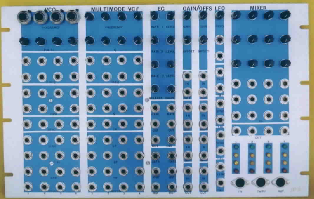
So, I have built a new panel for the top of the synth. The new modules that will go into are four VCO's. These VCO's will be what I have come up with in the way of temperature stabalized exponential converters. It is a relatively simple circuit, and I hope to have schematics up soon. There will also be 4 VCF's. These will be the standard state variable type that is fairly common (BP,LP and HP outputs). There will also be 4 multi segment envelope generators. There will also be two sets of quad gain/offset voltage processors. There will also be a quad LFO. The frequency control will be common for all LFO's, and each will have its own output and sync input. And finally, there will be a quad 3 in-> 1 out mixer.
I am also working on restoring the Paia
8700 keyboard I had originally purchased to control this
thing.
I am installing a Fatar keyboard into it.
Oct 1, 2000
Well, I am finally on my way to restoring the synth I built a little over 20 years ago. It hasn't been touched, probably, for about 15 years. Not since one of my cats got into it and chewed up the wiring. Anyway, besides fixing the stuff that was broken, it is also being documented by redrawing the board schematics with CAD (back then cad was unthinkable). It is being expanded. I am going to add more filters, four more VCO's, four more envelope generators, plus MIDI. When I stopped playing with this synth is about when Midi was first coming out.
CPU BOARD
Some things are going to be newly built, such as the CPU card. The CPU card is going to be based on the 68008 uP. It will be on a wire wrap card with oodles of ram and rom. It will be running a real time OS that I wrote. I hope to include simple sequencers and stuff like that in the thing. The hardware features of the CPU card are as follows:
1. 8 bit input port that
provides
interrupts for 4 trigger and 4 gate signals. Trigger signals
generate
an interrupt on it's positive transition. Gate signals can
generate
interrupts on both negative and positive transitions.
2. Two latched output ports
(PA and PB) which are used to control the Sample and Hold card for the
analog outputs. (4110 and 4120 boards). Also associated
with
these two ports is a strobe that will be generated after port PB is
written
to.
3. One set of standard midi
ports (IN, OUT, THRU).
4. One RS232 port.
5. One 8 bit input port for
use with a 16 channel A/D converter.
Hex Addressable Sample and Hold
There are two cards involved here. The 4110 board was a 16 channel sample and hold. The 4120 board, it's companion, had the DAC and some other glue logic. It was intended that one 4120 could control 4 4110 boards. I think someplace I still have some blank 4110's. These are actual real PCB's. They were taped up, again, this was long before CAD. Now, to tell you the truth, I am not really sure what I had intended to do with these. They were being installed when the above disaster struck, and that was when I lost interest. But, I will still make use of them. In fact, I should have a much easier time now that I am using a more powerful CPU and a RTOS.
4110
HASH board schematic
4120
HASH controller schematic
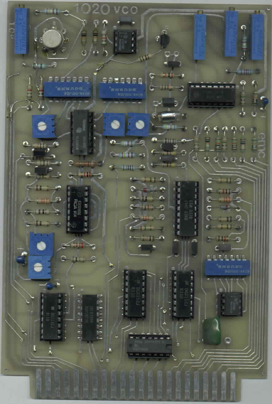
Voltage Controlled Oscillators
The original oscillators were built using individual parts (it's schematic is elsewhere on this web site as the old vco). It was replaced with a CEM3340 based oscillator. This was built on a printed circuit board, again, hand taped, in fact, any of the PCBs in this thing were hand taped. As far as I know, they still work (they did the last time I used the thing). Schematic to be posted soon.
Update.
I decided that I might as well rebuild the original VCO's that were in the synth. These were made on 3662 plug boards. I stripped of the VCO core and am replacing it with a circuit similar to the one on my SMB-1 board (which are similar to the ASM-1 VCO's). These will use my electronic temperature compensation. The wave shapers are going to remain the same.
Hopefully, this will work better than the original circuit did.
Voltage Controlled ADSR
These are still the
original
ADSR. I built these on a Vector 3662 plug board with a .156 inch
44 pin edge connector. It used a CA3080 as the control element,
and
of all things, I used a pair of CA3060's (triple CA3080) Ota's as the
multiplexors.
The logic was done with a LM339 comparator and diode logic.
Schematic
to be posted soon.
Voltage Controlled Amplifier/Mixer
Now this was sort of an
interesting
board. The original one was built on Vector 3662 plug
board.
I think I used CA3080's for the four VCA's. I had all four
outputs
connected together (thus a mixer). It was replaced by a PCBoard
version
later that used a pair of CA3280's instead. Schematic to be
posted
soon.
Voltage Controlled Filter
Originally, this synth only had one VCF (multimode). This was partly because of lack of panel space, and lack of space in the card cage. The original VCF was build using 3 CA3096 PNP/NPN transistor arrays. Two of the devices control the frequency and one controlled the Q. This was later replaced with a filter that used the CA3280. Schematic to be posted soon.
So, just what am I going to do?
Well, for one, a new panel is going to be added. It will provide space for more VCO's, more VCF's, more ADSR's and a few assorted goodies. The VCO is going to be a new VCO. I am working on a design that will hopefully be temperature compensated electronically. I still have not decided whether it will be a triangle VCO or a sawtooth VCO. Each have their own merits. Not matter which one is chosen, the final VCO will have the standard wave forms, and possibly maybe also divide by 2,3 and 4 outputs. I haven't decided.
The ADSR's are going to be something I built a long time ago. Again, I have no idea what I intended. I did not even remember building this circuit. But the thing has 4 channels, using CA3280's as the control element. Each channel has two inputs. One input controls the time constant, the other sets the voltage that the thing wants to ramp to. A comparator indicates when it has gotten to where it is going. It is supposed to be controlled by a micro processor. I am going to give it a whirl and see where it goes.
I still have not decided yet what I am going to do with the VCF's. But I do have an idea for generating controlled distortion, so I can set it up for a particular effect. I have no real idea if this is even feasible or not. But what the heck. I will only look like a fool if it doesn't work.
New Backplane for Synth Expansion
October 10, 1999
I just finished doing the new backplane
for my synth expansion. This backplane will also be used in
future
synths.
Why a backplane? Good question. This is not the first time I have used a backplane. But this is the most involved one. Even what is in the JP II right now is sort of a back plane. It consists of 44 pin edge connectors (22 x 2) mounted on rails. They are connected with wire. These connectors are not on a PCB but have solder eyelets. But the new backplane is a little bit more.
Backplane Features. The new backplane is going to have a scaled down microprocessor bus. It is 8 data bits wide, and has 10 address lines, the top four of which will be used to select the card. Four of the pins has encoded into it a unique pattern that can be used to identify each card (i.e. no need for a dip switch on the card). Each slot also has associated with it a 24 pin IDC connector. On this connector there are 20 lines from it's slot that can be used for any purpose. The idea here is that this connector will be used mostly to run wires to connections on the front panel. Being on a connector, it should be easy to disconnect the front panel from the electronics making it easier to work on. Also on the backplane are bus lines for downloading data to Xilinx Gate Arrays, an interrupt priority structure (cards closest to the CPU will have the highest priority).
Mechanical features are the slots are spaced at 1 inch. Card sizes can be either 4.5 x 6.5 inches or 4.5 x 9.0 inches. Oh, other sizes will work, of course, but these are the sizes that were intended.
Schematic
of Backplane. (pdf)
Printed
Circuit Board of Backplane (done with Protel for Windows 2.7, zip
file
of .pcb).
I am not sure when I can get these made. If you are interested, I will probably have a few spares when they are made. I have no idea how much the might be, but in the neighborhood around $50 (boards are 5" x 14").
New VCO's For Expansion
The original synth only had one VCO per voice. Well, I just couldn't afford any more back then. The new VCO card will be a dual VCO. Why dual? Well, for one thing the MAT-04's I plan to purchase make this convenient.
Also, way back when, the original VCO's were "discrete", in that they were built up from common components. Now, while the VCO did work, it wasn't great, especially in the thermal drift department. It was a heated exponential, and perhaps the temperature wasn't high enough or there was some other problem, but they did drift. Then I switch to CEM3340's, these worked great, but are no longer manufactured. So, it is back to discrete.
The first VCO I have decided to make a triangle VCO. Most people use an OTA for this, such as a CA3080 or LM13700, but I decided to use the THAT140 PNP/NPN pair array. The two PNP's are connected up as current mirrors and the two NPN's are connected up as a diff pair. This makes a simple OTA, although they way I am using it is more like a current switch.
The exponential converter will eventually be made from one pair in the MAT04 (one pair per VCO). But for the moment, since I can't afford them, the CA3046 will have to suffice. It has more emitter bulk resistance, but it should be adequate to prove the principles. Then comes the question of temperature compensation. The simplest method is to use the old Q81 (+3300ppm) resistor. The resistor must be in good thermal contact with the matched pair in order to work. This is difficult at best, and there will always be a little thermal lag. Although, in general, this is not much of a problem. Also, temperature control is another option. But this requires at least one extra transistor in the array to use as a heater, plus the current consumption of the VCO goes up dramatically. Another way to compensate is to use the leg of the exponential converter that is running at constant current as a thermometer and use this voltage to control an OTA to vary the gain accordingly. Originally I was going to put the OTA into the feedback loop of an opamp (this is required so that you can get 1/T). Juergen Haible then pointed out that by using the linearizing diodes of the OTA to control the gain, you get the 1/T without having to put the dang thing in a feedback loop.
So, what you will find here is a very, very preliminary schematic. It is basically just the core of the VCO's. Some things, such as SYNC, the ramp converter and the PWM section are still missing. I have almost got one half wired up to test. But I need to purchase a scope among other things before I can really start testing.
Preliminary
Schematic of Temperature Compensated Dual Triangle VCO(pdf)
Another Triangle
Oscillator
Yet Another Triangle Oscillator
Oct. 1, 2000
Here is another triangle oscillator design. This one, I am trying to get the advantages of the OTA triangle oscillator and the JFET switched oscillator. The disadvantages of the OTA triangle oscillator is that there is a slight temperature dependence introduced by the OTA. The harder you drive the OTA, the less this dependence, but that then creates other problems. The JFET switched oscillator eliminated the tempco problem but introduces a charge transfer problem. The charge transfer problem can be tweaked out.
The hope is that this circuit will have neither the temperature dependence or the charge transfer problem. It uses the same number of expensive transistor arrays as the OTA based triangle oscillator, although, because it needs three of the four transistors in a MAT04, this precludes doubling up the VCOs for a single MAT04 (dual VCO is out of the question in other words).
Yet Another Triangle Oscillator
This VCO as of Oct. 1, 2000, has not been tested, or built for that matter.